
連続超臨界水熱合成法
ナノ粒子開発
Nanoparticle development
各種ナノ粒子の開発
科学で、素材を生み出す。
アートビームは、独自の連続超臨界水熱合成法(Continuous Supercritical Hydrothermal Synthesis)を用い、さまざまな機能性ナノ粒子の研究開発・製造を行っています。電子・医療・環境・触媒分野を中心に、次世代のものづくりを支える素材づくりに取り組んでいます。

連続式 × 超臨界水 × ナノ粒子
超臨界水とは
(super - critical – water : SCW )
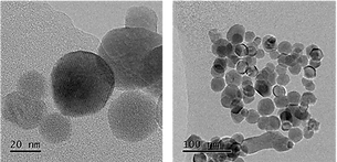
大気圧下において、水は0℃以下で氷に、100℃以上で水蒸気になります。このような固体・液体・気体の変化を相変化とよびます。水の場合、374℃、22.1 MPaを境として相変化が起こらなくなるため、この温度と圧力の条件を臨界点とよび、この臨界点を超える水を超臨界水とよんでいます。水の臨界点以上の領域でナノ粒子を合成する方法を超臨界水熱合成法とよびます。

連続式超臨界水熱合成法について
東北大学 ディスティングイッシュトプロフェッサー阿尻教授の発明で、地球上で見出される物質は、全てナノサイズの粒子として連続合成出来るという途轍もない可能性を秘めた技術です。すでに、海外でも先端ナノ材料製造を中心に実用化展開が急速に進んでいます。 弊社は、サポイン(戦略的基盤技術高度化支援事業)、NEDO(国立研究開発法人新エネルギー・産業技術総合開発機構)のプロジェクトを通じ、東北大学阿尻研究室様とこの連続超臨界水熱合成法を用いて長年共同研究を続けてまいりました。

連続式超臨界水熱合成法の強み
あらゆる物質をナノ粒子化可能
地球上に存在するあらゆる物質は、条件を適切に調整することでナノサイズの粒子として合成することが可能です。これにより、従来は困難だった物質の微粒子化や高機能化が実現され、用途に応じたナノマテリアルを提案いたします。
高温合成による優れた結晶性
高温環境下で反応が進行するため、粒子の結晶構造が非常に整った高結晶性のナノ粒子を得ることができます。結晶性の高さは、材料の安定性や機能発現に大きく寄与し、特に電子材料や光学材料の分野で重要な特性とされています。
狭粒径分布を実現する核生成制御
合成反応中に均一な核生成を制御することで、粒子の成長速度にばらつきが生じにくくなり、粒径の揃ったナノ粒子に。狭粒径分布の特性は、分散性や機能均一性を求められる用途において極めて重要であり、応用領域を広げます。
多元系・金属ナノ粒子にも対応
連続超臨界水熱合成法により、CuやAgをはじめとする金属ナノ粒子や複数元素を含む多元系粒子の合成が可能です。目的に応じた機能性粒子の開発に柔軟に対応しています。
研究機関・大学との豊富な実績
これまでに多数の大学・研究機関・企業の研究開発部門と連携し、各分野の専門的かつ多様なニーズに支援してきました。材料特性、スケール、応用目的に応じて柔軟に対応し、信頼性の高いパートナーとして評価をいただいております。

次世代を支える
ナノ粒子ソリューション
アートビーム株式会社R&D Centerでは、連続式超臨界水熱合成法を用いて、電気・電子部品材料、磁気材料、医療用材料、蛍光体材料、電極材料、触媒、高屈折材料など、幅広い分野で活用可能な革新的ナノ粒子の研究開発と製造を行っています。次世代のニーズに応える新しい特性を備えた“新機能製品”の創出に向けて、貴社の技術開発を力強くサポートいたします。
積層セラミックコンデンサ
チタン酸バリウム カルシウム ジルコニウム(BCTZ)
自然歯のような人工歯材料
イットリア安定化ジルコニア(Y-ZrO2)
サーモクロミックウィンドウ
二酸化バナジウム(VO2)
軽量、薄型レンズ 高屈折材
イットリア安��定化ジルコニア(Y-ZrO2)
開発事例
BCTZ
・化学式(Ba ,Ca)(Ti ,Zr)O3
・チタン酸バリウム(BaTiO3)に酸化カルシウム(CaO)と酸化ジルコニウム(ZrO2)�を複合化

BNT
・化学式(Bi0.5 , Na0.5)TiO3
・チタン酸ビスマス ナトリウム

VO₂-W
・化学式 VO2
・二酸化バナジウム(VO2)に酸化タングステン(WO3)を複合化
世界にまだ無い
機能のナノ粒子が欲しい
量産化を見据えた試作も柔軟に対応いたします。お気軽にご相談ください。本技術の詳細は以下ダウンロードページよりご覧いただけます。


